pcb course class 11 images 94v Circuit Diagram Learn how to design your own PCB step-by-step, from creating a schematic to building a board. Find out the best PCB design software, materials, and manufacturers for your project.
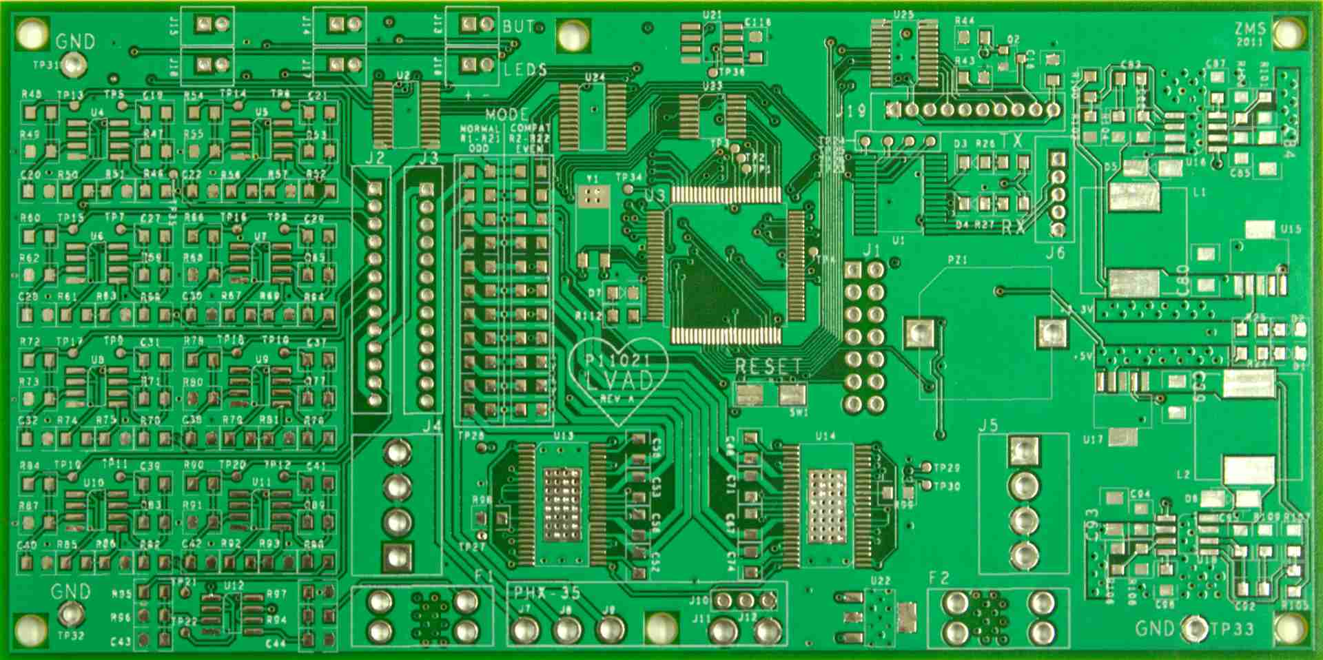
When finished drawing the board, it is time to get your PCB design ready for manufacturing. This basically means you need to check your board for errors and convert your board layout to Gerber files. Then, choose a cheap PCB manufacturer and get your board made. We have used EasyEDA PCB manufacturing service to manufacture the example PCB. What is a PCB and Intro to PCB Design Printed circuit board (PCB) design has grown into its own specialized field within the electronics industry. PCBs play an important role in that they provide electrical interconnections between electronic components, rigid support to hold components, and a compact package that can be integrated into an end Learn the steps to design and make your own PCB from a circuit diagram. Find out how to use KiCad software, choose components, order PCBs, and solder them.
Your Guide to PCB Design Basics & Steps Circuit Diagram
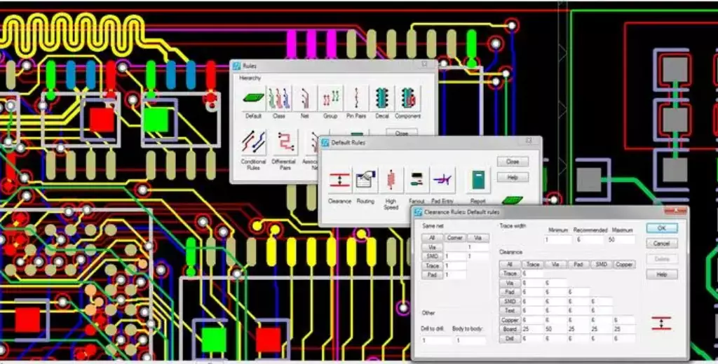
4. Design your PCB stackup. This is important to consider early on in the PCB design stage due to impedance, which refers to how much and how quickly electricity can travel down a trace. The stackup plays a role in how the mechanical engineer can design and fit the PCB into the device. 5. Define design rules and requirements.
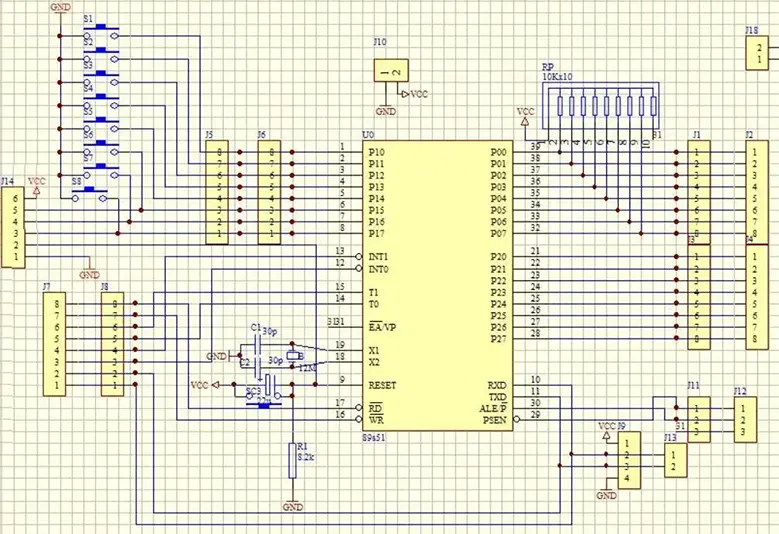
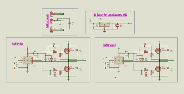
Larger circuits can be difficult to design on a single layer PCB. As design complexity increases, it gets harder to route the traces without intersecting one another. Luckily there are double, triple, and multi-layer PCBs that allow traces and planes to be routed on electrically isolated layers. STEP 1: Take a printout of circuit board layout. Take a print out of your PCB layout using a laser printer and the A4 photo paper/glossy paper. Keep in mind the following points: You should take the mirror print out. Select the output in black both from the PCB design software and the printer driver settings. Step-by-Step PCB Design Tutorial for Beginners. Designing a PCB involves a series of steps to ensure the final product works as intended. There are a number of websites that allow to create online PCB design. Here is a simple and easy-to-follow step-by-step guide for beginners: Step 1: Schematic Design. This is the blueprint of your PCB.
PCB Design: How to Create a Printed Circuit Board From Scratch Circuit Diagram
Step 2: Create a Blank PCB Layout . Next you're going to create the layout where your schematic is going to come to life. Create a PcbDoc File: Open up a new PCB document in your CAD tool. Define Board Outline: Shape and dimension the board according to the needs of the project. Create Gerber Files in KiCad. From the PCB Editor in KiCad you can create Gerber files by going to the File menu and selecting Plot… A window will appear. Click on the Plot button to create the Gerber files. To create Drill files, click on Generate Drill Files… to open the Drill File dialog. Then click the button Generate Drill File.