DIY Buck Converter 3 Steps Circuit Diagram How to Design a Buck Converter | Power Supply Design Tutorial | Buck Converter Design TutorialThis is a complete tutorial on how to design a synchronous buck Therefore, the Buck converter is chosen as the design because it meets all of the specified criteria. Then, the basic circuit topology of the Buck converter, which includes five standard components: (1) a pulse-width modulating controller, (ii) a switch, (iii) an inductor, (iv) a capacitor, and (v) a diode.
That's enough theory; now let's examine a straightforward real-world circuit. Making a Practical Buck Converter Design. The following figure shows a simple practical DC to DC buck converter circuit using only 3 transistors and a few other passive elements. It works in the following manner: Switch S in this circuit is represented by transistor T1. Buck Converter: Types, Circuit Design, Modes of Operation, Examples, Losses and Applications. Design of Buck Converter for 12V to 2.5V 1A. The basic buck converter consists of a controlled switch, a diode, capacitor and controlled driving circuitry. The switch controls the flow of input power into output by turning ON and OFF periodically.

Simple Buck Converter Circuits using Transistors Circuit Diagram
Buck Converter Basic Function. Before going to buck converter design tutorial, we will discuss first how buck converter works in order to fully understand the following tutorial. A buck converter is a switching converter with a voltage output lower than voltage input. It is also called as a step-down switching converter Buck Converter Block Diagram and General Thoughts. Among the switched-mode power supplies (see DC-DC Converter Basic Characteristics and Formulas), the buck converter (step-down converter) is certainly the most widely used topology. The buck converter is basically nothing more than a square wave generator with a downstream LC filter.

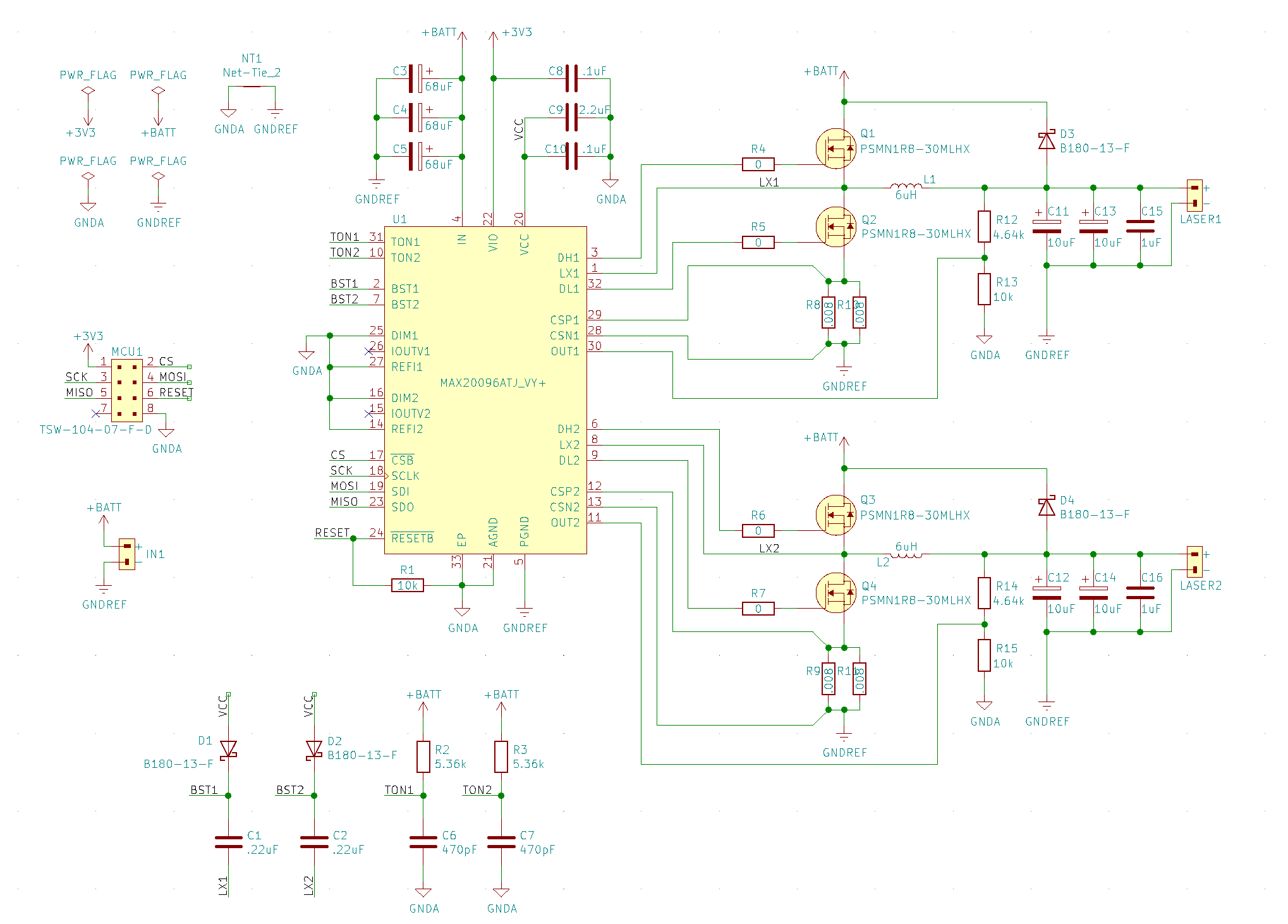
Circuit diagram of a buck converter. A basic buck converter comprises essential components like a switch (MOSFET or BJT), an inductor, a diode (or a second MOSFET), and a capacitor, as depicted in Fig 2. To design a buck converter, it is essential to determine the values of the capacitor, inductor, diode size, and switch size. The following The basic components of the switching circuit can be rearranged to form a step-down (buck) converter, a step-up (boost) converter, or an inverter (flyback). These designs are shown in Figures 1, 2, 3, and 4 respectively, where Figures 3 and 4 are the same except for the transformer and the diode polarity.

Circuit, Design, Operation and Examples Circuit Diagram
The working principle of a Buck Converter involves the conversion of a higher voltage to a lower voltage through a series of switches, inductors, and capacitors. The basic operating principle of a Buck Converter is as follows: The input voltage is connected to a switch (usually a MOSFET), which is controlled by a control circuit. A typical buck converter circuit is shown in the above image. It's quite similar to a boost converter, but the placement of the inductor and transistor are switched. The switch shown in the above circuit will normally be a power electronics switch like MOSFET, IGBT or BJT. The switch will be switched (turned on and off) by using a PWM signal.